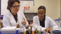
- Surya Nalamati
- Research assistant
- “EAGER Self-Catalyzed Growth of Patterned GaAsSb and GaAsSbN Nanowires for Optolectronic Devices”
- http://eceserver.ncat.edu/iyer/
- North Carolina A&T State University
- Ashlee Gordon
- “EAGER Self-Catalyzed Growth of Patterned GaAsSb and GaAsSbN Nanowires for Optolectronic Devices”
- http://eceserver.ncat.edu/iyer/
- North Carolina A&T State University
- Roderick Gray Jr.
- Undergraduate Research Assistant
- “EAGER Self-Catalyzed Growth of Patterned GaAsSb and GaAsSbN Nanowires for Optolectronic Devices”
- http://eceserver.ncat.edu/iyer/
- North Carolina A&T State University
- Dennis Hernandez
- “EAGER Self-Catalyzed Growth of Patterned GaAsSb and GaAsSbN Nanowires for Optolectronic Devices”
- http://eceserver.ncat.edu/iyer/
- North Carolina A&T State University
- Shanthi Iyer
- http://jsnn.ncat.uncg.edu/faculty/shanthi-iyer-ph-d/
- Research professor
- “EAGER Self-Catalyzed Growth of Patterned GaAsSb and GaAsSbN Nanowires for Optolectronic Devices”
- http://eceserver.ncat.edu/iyer/
- North Carolina A&T State University
- manish sharma
- Research assistant
- “EAGER Self-Catalyzed Growth of Patterned GaAsSb and GaAsSbN Nanowires for Optolectronic Devices”
- http://eceserver.ncat.edu/iyer/
- North Carolina A&T State University
Public Discussion
Continue the discussion of this presentation on the Multiplex. Go to Multiplex


Louis Gross
Director and Professor
Surya et al.,
Thanks for an interesting comparison of nanowire development to that of grass growth. Can you say a bit more about how this project developed particularly what are the major challenges in growing nanowire? Also, what are the new opportunities in photonics that nanowires can foster?
Cheers,
Lou
Surya Nalamati
Research assistant
Dear Dr. Louis,
Thanks for your interest.
We have a well-established group on arsenide-antimonide based thin film structures grown by molecular beam epitaxy. In the past five-six years, our group has expanded our research work to the synthesis of these materials in nanowire configuration for photodetector applications.
Preparation of the substrate was found to be the most critical for the nanowire growth. Overall, nanowire growth is challenging as the growth parameter space that requires optimization is larger than those in thin films and due to complex interdependency between the effects of different growth parameters. Further, in antimonide based nanowires, the low solubility and low supersaturation of Sb in the seed melt also poses a greater challenge to the growth.
One dimensional nanowire geometry offers unique changes to the properties of the materials, greater optical trapping, larger freedom in the material combination and diverse device design architectures. These positive attributes can be exploited to significantly improve the performance of optoelectronic devices namely, nanoscale lasers, photodetectors, solar cells along with their heterogeneous integration on the silicon substrate. For instance in detectors, the performance of the photodetector can be pushed to a single photon limit for optical quantum information applications and in solar cells, the efficiency closer to Shockley Quiesser efficiency limit can potentially be reached.
Louis Gross
Director and Professor
Surya, Thanks for the detailed response. Great to know there are many opportunities for the use of nanowires.
Courtney Arthur
Thanks for sharing your project. I am curious what challenges you have encountered thus far and what ways you have found successes in your work?
Surya Nalamati
Research assistant
Dear Courtney,
Preparation of the substrate was found to be the most critical for the nanowire growth. Overall, nanowire growth is challenging as the growth parameter space that requires optimization is larger than those in thin films and due to complex interdependency between the effects of different growth parameters. Further, in antimonide based nanowires, the low solubility and low supersaturation of Sb in the seed melt also poses a greater challenge to the growth.
We have carried out a very systematic work to find the effect of each growth variant and extensive characterization to get a better understanding of the growth kinetics. These studies enabled us in coming up with some unique growth parameter variations such as two-step growth temperature, the variation of the constituent fluxes during the growth to grow high-quality vertical nanowires of desired composition and properties.
Dave Barnes
Associate Executive Director
Surya and team,
Very interesting! Though it's clear that I have a lot to learn in this area. I appreciate your use of analogies to help convey the work that you do. One area I'm interested in is how we can use mathematics and statistics to give students insights into interesting science and the work of interesting scientists. I'm wondering if as you think about your work there are any ways math or stats could be used as a path to understand the project?
Surya Nalamati
Research assistant
Dear Dave,
This is a very interesting question. Yes, both mathematical modeling and statistics would be very useful in advancing the fundamental understanding of the growth kinetics as explained below.
One of the issues with the nanowires is the inhomogeneity in the physical dimensions amongst the nanowires and their properties. A statistical analysis of the distribution of size and shape of the seed droplet in the initial stages of the growth as well as the dimensions of the nanowires after the growth as a function of growth parameter variations would provide a better insight and optimization of the growth.
A good mathematical modeling of the growth is really required that would provide better understanding of the impact of growth temperature and various constituent elements on the adatom mobility, surfactant effect, surface energy, all of which affects the growth kinetics. The successful modeling would really assist in coming up with novel approaches to growth.
Further posting is closed as the showcase has ended.